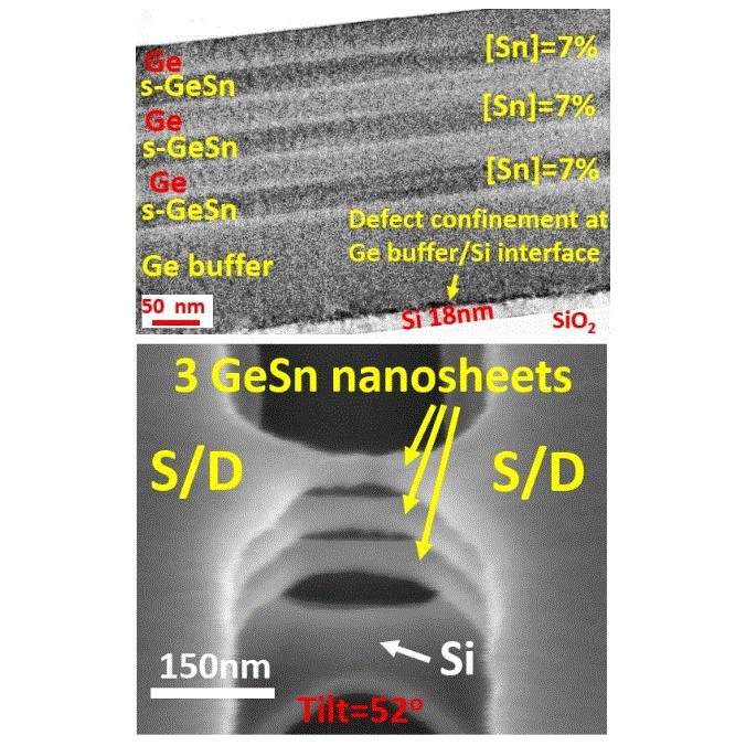
High-quality, fully compressively strained CVD-grown GeSn multi-layers are produced with defects confinement near the Ge buffer/Si interface. With the Ge layers used as sacrificial layers, the optimum ultrasonic-assisted H2O2 etching technique, the low thermal budget gate stack (400 °C), and the S/D parasitic resistance reduction, the first stacked 3-Ge0.93Sn0.07-nanosheets pGAAFET with LCH = 60 nm achieved record high Ion=1975μA/μm per channel width among all GeSn pFETs. Uniform stacked GeSn nanosheet GAAFETs with low surface roughness are compatible with Si technologies and are good candidates for future technology nodes to extend Moore’s law for CMOS scaling.
Research
Research areas of Professor Chee Wee Liu (Distinguished/Chair Professor of NTU)
- SiGe/Ge/GeSn epi technologies for the more Moore and more than Moore applications, including 3D stacked high mobility channel transistors, related gate stack, and Si photonics (Lidar/IR detector/ CMOS image sensor).
- Mobility/transport calculations, band structure calculation, First principle calculation.
- Memory technologies : MRAM and DRAM.
- High mobility IGZO TFT and Si solar cells
Novel Electronics
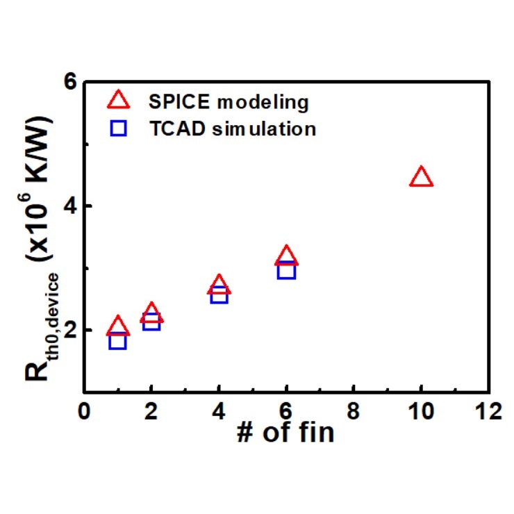
Self-heating effect of the 3D transistor is simulated by TCAD. The boundary/alloy scattering and the nanostructure effect are considered. From the results, the device thermal resistances are extracted. In addition, thermal SPICE modeling for the 3D transistor is proposed and verified by the TCAD simulation. Our modularized thermal SPICE model has dependencies on the device geometries, materials, and layouts. It provides frequency-dependent spatial and temporal temperature distribution. Thanks to its less computation cost than the TCAD simulation, the self-heating effect and related reliability issues of small circuits (e.g. 5-stage ring oscillators) are evaluated by our SPICE model.
DRAM
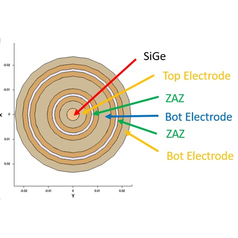
TCAD simulation of DRAM capacitor is being developed. The fabrication of DRAM capacitor optimize process condition for DRAM 1x node scaling. Analysis and measurement are used for the reliability issue of DRAM capacitor.
In the past years, there has been increasing interest in amorphous indium gallium zinc oxide (a-IGZO) thin-film transistors (TFTs) for Active Matrix Organic Light Emitting Display (AMOLED). The a-IGZO TFTs have higher on/off current ratio (~108) and higher carrier mobility (~28 cm2/ (v-s)) as compared to amorphous Si (a-Si) TFTs, and is suitable for the high performance applications.
In-situ doping by chemical vapor deposition (CVD) has been reported as an efficient method to simultaneously achieve high active dopant concentration and high crystallinity for B-doped GeSn on Ge-buffered Si at low growth temperature of 320oC. To further increase the active dopant concentration and Sn content simultaneously, the epitaxial growth temperature < 320oC by CVD is performed. At 320oC, the growth rate of B-doped strained GeSn is 24x enhancement as compared to undoped Ge. By lower the growth temperature to 305oC and 290oC, the active [B] of 4.9x1020 cm-3 and [Sn] of 14.2% are achieved, respectively. The low contact resistivity of 2.4x10⁻⁹ Ω-cm2 for in-situ B-doped epi-GeSn by CVD is demonstrated.
The thermal model of spin-transfer torque MRAM (STT-MRAM) is being developed. The self-heating and the thermal coupling between transistor and magnetic tunnel junction (MTJ) can increase the MTJ temperature. The increasing temperature leads to the degradation of read disturbance and MgO reliability.
BSIM and Mextram models are being developed to take the strain and optical effects into account for RF and high speed digital applications. Finite element analyses of ISE-TACD and ANSYS are used to simulate Ge FET and MOS LED/GOI detector theoretically.
Photonics
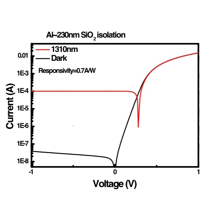
The bandgap tuning and direct bandgap emission of GeSn can enhance the performance of group IV photonic devices on Si platform.
BSI cmos image sensor with NIR detection can be used in the camera and automobile applications.
Optical steering can achieve by optical phase array. This technique can be used for the Lidar applications.
Photovoltaic
Quantum efficiency (QE), solar cell efficiency, dark and photo I-V measurement, carrier lifetime measurement by QSSPC, and FTPS for defect level.